
Designing the fit between PCBAs and mechanical assemblies: often overlooked.
There are two common issues associated with designing and manufacturing products that have PCB (printed circuit boards) in them:
- Fitting of the electronics in the box or its associated mechanical assembly
In among the challenging and fascinating digital signal processing, sensitive signal analysis, advanced firmware, etc. the problem of making sure the PCBA (assembled PCB) will fit seems trivial: so sometimes no one does the groundwork. The product is made, and the PCB will not fit in the box! This is a disturbingly common outcome. Delays, frustration and unnecessary costs ensue.
- Physical/mechanical constraints on the PCB
You want to design a product. Do you get the product designer to design the mechanics and tell the electronics supplier what size and shape the PCB needs to be, or vice versa? It is a real chicken and egg situation, and it is amazing how often it results in indecision and stalled projects. Those involved can behave like rabbits in headlights. The answer to this dilemma is that if an optimum is being sought (size, aesthetics), there is no choice other than to iterate until the requirements of the electronics and the enclosure come together (multiple prototypes, more expensive); but if the expectations are just a little lower, do the PCBA first and make the mechanics fit around it.
It is almost always possible to recover from omissions relating to the fit of mechanics and electronics, but time and some money will be wasted. It is impossible to recover this time!
Fitting the Electronics into its Enclosure/Box/Mechanical Assembly
Let's assume that the mechanics follow the PCBA as is most commonly the case, and that the mechanics are going to be designed and made by a third party (I'll go into the types/options for enclosures later in this post).
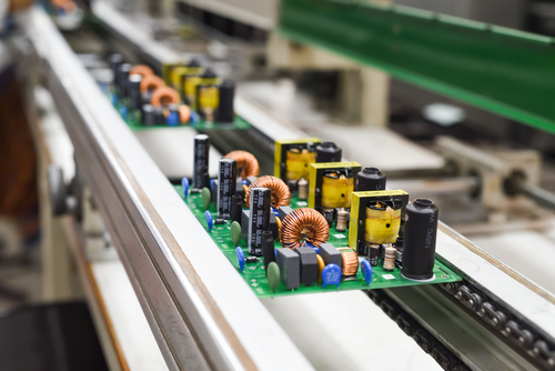
In order for the PCBA to fit its enclosure (box or space that it must fit into) it is necessary to specify the dimensional limits before the PCB CAD layout is done. CAD layout, done with products like Altium or Easy PC, is the process by which the PCB shape, thickness, tracking, etc. are specified so that PCBs can be manufactured.
What are the Physical Constraints on the PCBA?
(PCB with components assembled onto it)
There are a number of things to consider when designing a PCBA to fit into something else, as it will invariably do:
- The dimensional constraints on the board shape (.dxf file)
If presented with a situation in which the mechanical authorities are dictating that the PCBA must fit into a given volume, it is entirely reasonable that your response is to dictate that they provide you with a precise description of that volume. The .dxf file is a way for the mechanical engineers to do this. It is a file/drawing that defines, to scale, the 2D dimensions of a space. It can be imported into PCB CAD packages to form a PCB outline and precisely define connector positions and other important dimensions, e.g. the position of fixing holes. The third dimension can be incorporated into it by having the mechanical engineers define height limits on the 2D drawing. You must get this or something equivalent from the mechanical engineers: How else are you to know what size your PCBA needs to be?
- Placement reviews of the PCB layout (datums; tolerances on, for example, fixing holes)
Have a 'Placement Review' with all the technical team members. This is the stage at which the board outline has been decided, all components that are in fixed positions have been defined, and all components are placed on the board, but no tracks have been laid. The kind of things that should be discussed and approved are: checking that appropriate datums have been used (avoid building up cumulative errors through poor dimensioning); check that everything has a realistic tolerance (if a 2mm hole through which a 2mm diameter shaft will fit is required, it is no use specifying a hole of 2mm - very common error, and I'll leave the reader to work out why); check that all things that align with the enclosure (screens, switches, connectors) are in the right position. There are numerous things that can be checked, and for the sake of rigor, it may well be a good idea to make a tick list.
- The thickness of the board and its height (including component profile - 3D render)
Most PCB CAD packages will allow the creation of a 3D image of a design. It is well worth doing this because it brings the design to life in a way that is impossible with 2D images and representations. It will help you and your team identify issues earlier. I recommend it is generated and is made an agenda item for the Placement Review.
- Checking the model using 3D prints
The relatively recent arrival of 3D printing in prototyping has completely changed the mechanical design process, but it also has a very useful spin off for PCBA design - you can 3D print your design to get a scaled, physical model of your PCBA! This is brilliant because it allows a check for whether or not your PCB will fit its mechanical assembly long before you've finished your design (PCB tracking, generation of manufacturing files and manufacture itself still to do). It is not an absolute check, but it will give a good deal of confidence. In 24 hrs it is possible to find out if the mechanics of the PCBA are essentially right, and you can pass a physical model to the mechanical team for them to check that it fits where and how it should.
- Use of CAD to verify fit (.igs files and Solid Works)
Once the placement review is completed, it is possible to create a step or .igs file that the mechanical team can introduce into its CAD, e.g. Solid Works, and thereby check that the PCBA fits into the mechanical assembly. I strongly recommend that this is done.
- Other contributors (conformal coatings, cables and their bend radii)
Conformal coating is the encapsulation of a PCBA in a thin plastic coating with high dielectric strength and good mechanical properties (it can protect against things like moisture). The thing is it does make the PCBA slightly bigger, so watch out for this. Areas of the PCBA can be masked so that that they don't receive the coating, but make sure those that do don't affect the fit, e.g. fixing holes getting coated and then not allowing shafts to pass through them. Another thing to watch out for with conformal coats is the fact that making modifications to the PCBA after coating is difficult, or impossible. More will follow on conformal coats in future posts.
Don't forget about access and the bend radii of cables when allocating space for your PCBA. It always takes more space than you might imagine. If you lack the experience to know how to allow for this, make a model and make your decisions on the basis of experiment, or talk to someone who has more experience. This is an involved topic and I think that I'll devote a post to it in the not too distant future.
- Heating and ventilation
Design incorporating thermal considerations is a topic in its own right, and it is covered on reputable degree courses (more on this in a future post), but it does bear mentioning hear. Has adequate ventilation been allowed for your PCBA, and does the maximum service temperature pose a threat to the integrity of your design?
- Safety/earthing/telecommunications
Is the mechanical assembly that houses the PCBA metal? Does the PCBA handle dangerous levels of electrical energy? If the answer to both these questions is yes, then it will be necessary to earth said metal casing. There are international standards to cover this sort of thing, which I don't think there's space to go into here, but I would like quickly to cover the concept of 'Single Fault Conditions'. If any single fault, relating to the integrity and management of potentially dangerous levels of electrical energy, can result in a hazard to a human, then your design will not pass the standards. This is where the concept of double insulation comes from. Another point to consider is radio frequency communications. If the design transmits the same, and is totally enclosed by metal - it isn't going to work very well.
Finally, there is another issue to be aware of - ESD (electrostatic discharge). There is a nasty little device that test houses use to confirm designs are capable of withstanding ESD, and this thing sits at approximately 6kV (voltage varies according to application) and the testers will touch any exposed metal part of your product with this nasty device. Make such a device isn't going to damage your design.
- Intrinsic safety
Just a quick note here (huge topic). Intrinsic Safety is all about making sure a design is not subject to fire or risk of exploding. It is covered by standards (ATEX). If your device falls into this category, one way of protecting it, and human life, is to install the PCBA in an ATEX qualifying enclosure, which will not allow, for example, flammable gases to enter it. That's all that I'm going to say on this in this post, but be aware of it if your PCBA and design could fall under this standard. Obviously, the reason for the standard is that a PCBA might be such that it can become an ignition source.
- IP ratings
Dust and moisture ingress in relation to mechanical assemblies and enclosures are covered by what is known as an IP rating. Make sure your know the requirements for your device, or establish them if there are none, and then make sure your design meets an appropriate IP level. You can find out about it from the web. Note your application may not require this - but knowledge of it helps.
- Prototyping methods (rapid prototyping, 3D printing, machining, standard enclosures, folded plastic, etc.)
This bullet point doesn't really have much to do with making PCBAs, but it is as well to be aware of the techniques that the mechanical team may use to cover its responsibilities in the realisation of the product.
Rapid prototyping involves the use of a silicone mould, which will become useless after it has made about 20 units, to produce prototype mechanical parts, in plastic. It is nothing like as popular as it used to be because of the advent of 3D printing, but it is quicker if the requirement is for tens rather than single digit numbers of prototypes (probably).
3D printing is entering its heyday. From a step file, the prototype is extruded layer by layer (very fine layers <0.1mm are available). It does take time for the machine to run, but it lends itself to be being left on overnight.
Machining is exactly what it says. Plastic or metal prototypes are machined from solid material. This leads to very high-quality prototypes, but they are almost certainly not comparable with the final item (injection mould for example).
Don't overlook that which can be bought off the shelf, and may well come with all the approvals required. I'm alluding to 'Standard Enclosures'.
Folded Plastic enclosures and metal enclosures (e.g. anodised aluminum) are a useful halfway house between standard enclosures and an injection moulded product. There are numerous turning and milling companies that can make the metal examples for you, and CDT in Bracknell can make folded plastic enclosures, which can look quite good and the crippling costs of tooling don't apply to them.
- EMC (metallic spray coatings)
Metallic sprays are available to provide electromagnetic screening on an enclosure or device.
- Feasibility for assembly
Design for Manufacture is a topic in its own right, but make sure that you have considered that some poor soul might have put together thousands of examples of your product. If you haven't really thought about it and tried an adequate number of prototypes in an appropriate manufacturing environment, you degrade the quality of your design, it will not last as long and it will cost more.
I hope all this has been useful. If there are any questions or you require prototypes, please don't hesitate to contact Newbury Innovation Ltd.